
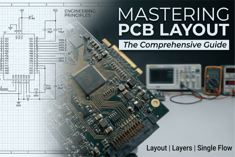
A PCB that works perfectly on a schematic can fail on a physical board. The layout determines everything: how signals travel, where noise enters, and whether the board survives production. Understanding PCB design basics is not just useful for engineers starting; it is essential for anyone responsible for a product that must perform reliably across real operating conditions.
This post covers the PCB design process from first principles: what the layers do, how signal flow shapes routing decisions, and which PCB design rules separate boards that work from boards that do not.
What Is PCB Layout Design?
PCB layout design is the process of translating a schematic diagram into a physical board. The schematic tells you what is connected. The layout tells you where everything sits and how copper traces carry signals between those connections.
The two are not interchangeable. A clean schematic does not guarantee a clean layout. Component placement, trace routing, layer stack-up, and copper pour decisions all affect whether the board functions as intended or introduces noise, crosstalk, and signal integrity problems.
This is where the PCB design process becomes a discipline, not just a drafting exercise.
How PCB Layers Work
Every PCB is a stack of conductive and insulating layers bonded together. The number of layers determines how much routing space is available and how well the board manages power and signal separation.
A single-layer board places all the copper on one side. A double-layer board adds copper on both sides. Multi-layer boards (four, six, eight layers or more) interleave signal layers with dedicated ground and power planes.
The ground plane is not decoration. It provides a low-impedance return path for every signal on the board, suppresses electromagnetic interference, and stabilises voltage across the design. Designs that omit a dedicated ground plane almost always exhibit signal integrity issues that are expensive to diagnose and difficult to fix without a board revision.
For both mixed-signal and high-speed digital designs, a four-layer stack (signal, ground, power, signal) is the practical minimum for predictable performance.
Signal Flow and Trace PCB Design
Signals do not simply travel from point A to point B. They follow the path of least impedance, and every trace on a PCB is a transmission line with electrical properties that depend on its width, the dielectric material beneath it, and its distance from the nearest reference plane.
Trace width controls current-carrying capacity and impedance. A trace that is too narrow for its current load generates heat and can fail. A trace with uncontrolled impedance on a high-speed line causes reflections that corrupt data.
PCB routing techniques that protect signal integrity include:
- Keeping high-speed signal traces short and direct
- Routing differential pairs with matched lengths and consistent spacing
- Avoiding right-angle bends (45-degree corners or curved traces reduce impedance discontinuities)
- Never routing signal traces directly beneath connectors or across split planes
- Keeping analogue and digital signal paths physically separated
The schematic diagram of the PCB transition is where these decisions begin. Net classes assigned at the schematic stage allow the layout tool to enforce width and spacing rules automatically during routing.
PCB Design Rules That Govern Every Board
PCB design workflow rules are the constraints that prevent electrical failures, manufacturing defects, and signal problems before the board reaches fabrication. Design rule checks (DRC) inside CAD tools verify compliance automatically, but the engineer must set the correct rules in the first place.
Core PCB layout guidelines include:
- Clearance rules: minimum spacing between copper features to prevent shorts and arcing under voltage
- Via design: via diameter and drill size must match the fabricator’s capabilities; blind and buried vias increase cost but reduce layer count requirements
- Component orientation: align passive components in consistent orientations to simplify automated optical inspection (AOI) and soldering
- Thermal relief: connect power pads to planes using thermal spokes rather than solid copper to allow controlled soldering and rework
- Silkscreen clearance: keep reference designators and polarity marks clear of pad areas so they remain legible after soldering
IPC standards (published by the IPC trade association) provide widely referenced benchmarks for PCB design rules, including minimum annular ring sizes, conductor spacing, and solder mask clearances. Following these standards gives fabricators a clear specification to work against.
PCB Design Steps: From Schematic to Manufactured Board
The PCB design steps follow a defined sequence. Skipping or compressing any stage typically creates rework later.
- Schematic capture. Define the electrical netlist. Assign component footprints at this stage, not as an afterthought.
- Board outline and constraint setup. Set the physical dimensions, layer stack-up, and all design rules before placing a single component.
- Component placement. Place components by function: keep high-speed ICs close to their decoupling capacitors, group connectors at board edges, and position thermal mass away from heat-sensitive parts. Placement drives 80 percent of routing quality.
- Routing. Route power and ground first, then high-speed signals, then general signals. Use copper pours for power planes rather than manually routed power traces wherever the design allows.
- Design rule check. Run DRC repeatedly during routing, not only at the end. Catching violations early costs far less than finding them after Gerber generation.
- Gerber file generation and fabrication review. Export fabrication files and review them against the fabricator’s capability sheet. Confirm drill files, layer order, and impedance-controlled stack-up specifications match the order placed.
Common Mistakes in PCB Design for Beginners
PCB layout guidelines exist because the same errors appear repeatedly across designers at every level.
Placing decoupling capacitors far from the IC they serve is one of the most common. A decoupling capacitor separated from its supply pin by several millimetres of trace is largely ineffective at high frequencies. The inductance of the trace between the cap and the pin negates the capacitor’s function.
Splitting a ground plane under a high-speed signal trace is another. When a signal crosses a gap in its reference plane, the return current must travel around the gap, creating a loop that radiates noise and degrades signal integrity.
Skipping the DRC before generating Gerbers is a third. Design rule violations that appear trivial in a layout tool can cause shorts, opens, or fabrication failures on the physical board.
And underestimating thermal management. High-current components and power regulators need copper pours, thermal vias, or heatsinks specified at the layout stage. Adding them after the fact often requires a board respin.
Building Reliable Electronics Starts at the Layout Stage
The PCB design process is where electrical performance is either protected or compromised. A well-structured layout that respects layer design, signal flow, and design rules produces boards that behave predictably, pass testing the first time, and hold up across production volumes.
MicroLOGIX designs and manufactures PCBs for OEMs across industrial, automotive, and embedded control applications. If your next product requires a design that meets both performance and production requirements, speak with MicroLOGIX’s engineering team about end-to-end PCB design and manufacturing support.
FAQs
- What are PCB design basics?
PCB design basics cover schematic capture, component placement, layer stack-up, trace routing, and design rule checks. These steps define how a board performs electrically and in production.
- What is PCB layout design?
PCB layout design converts a schematic into a physical board. It defines where components sit and how copper traces connect them across one or more conductive layers. - What are the main PCB design steps?
The steps are: schematic capture, board setup, component placement, routing, design rule check, and Gerber file generation. Each step must be completed before the next begins. - How many layers does a PCB need?
Nearly all digital designs use four layers minimum: two signal layers and dedicated ground and power planes. Simple analogue boards can work on two layers; high-speed and RF designs often need six or more. - What are PCB design rules?
PCB design rules are constraints on trace width, copper clearance, via size, and pad geometry. They prevent electrical shorts, manufacturing defects, and signal integrity failures. - What is trace PCB design?
Trace PCB design refers to routing copper conductors between component pads. Trace width, length, and impedance control determine how well signals travel across the board without distortion. - What are the best PCB routing techniques?
Route differential pairs with matched lengths, keep high-speed traces short, avoid right-angle bends, separate analogue and digital routing paths, and never route signals across split ground planes. - How do I go from a schematic diagram to a PCB?
Export a netlist from the schematic tool, import it into the PCB editor, set design rules and layer stack-up, place components by function, then route traces from power nets to signal nets. - What is PCB layer design?
PCB layer design defines how conductive and insulating layers are stacked. Layer order, thickness, and material affect impedance, signal return paths, and power distribution across the board. - What should beginners know about PCB design?
Place decoupling capacitors close to IC supply pins, use a dedicated ground plane, run DRC before exporting files, and match trace widths to current and impedance requirements from the start.