
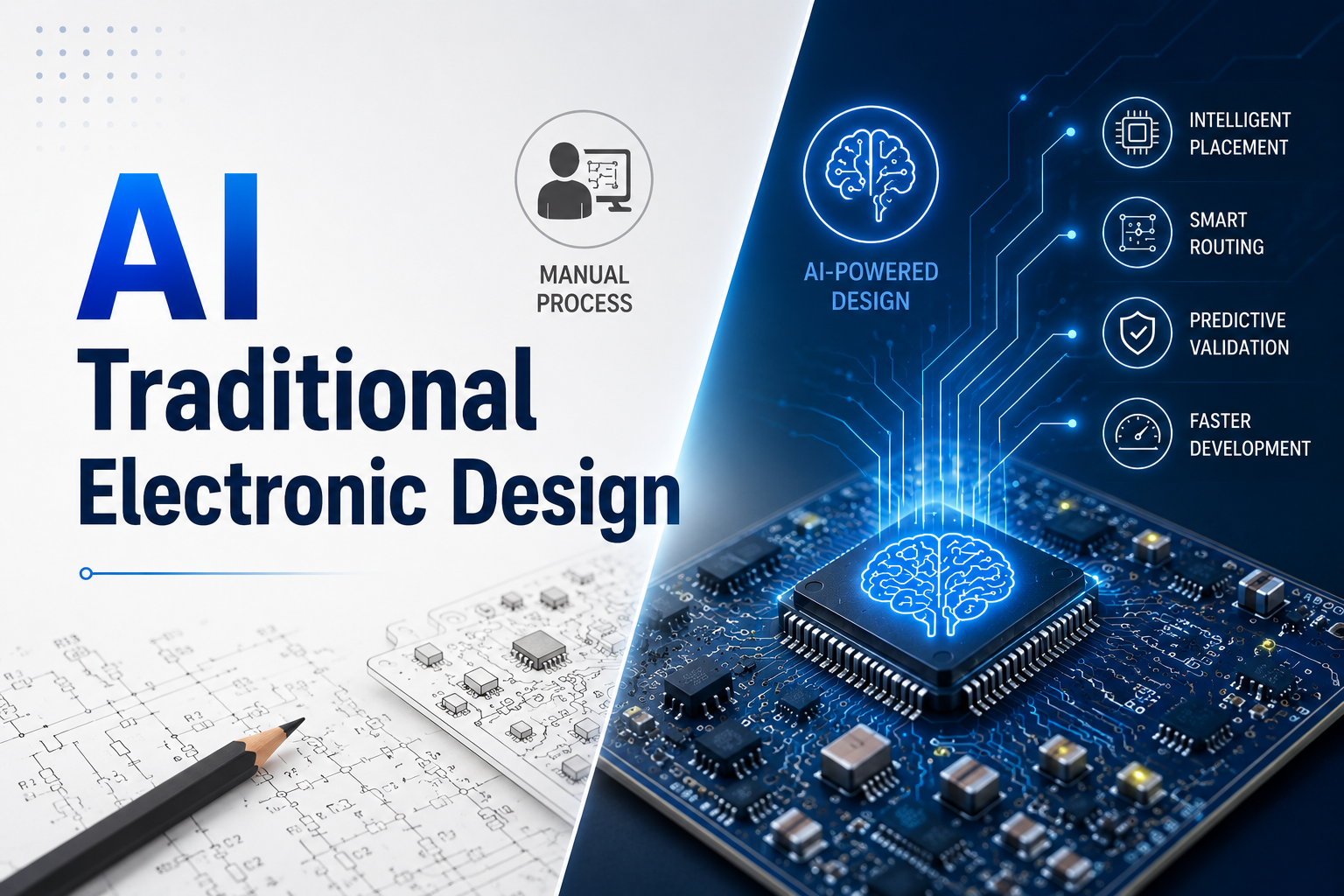
Artificial intelligence is reshaping industries at an unprecedented pace, and electronics engineering is no exception. For decades, engineers relied on experience, engineering judgment, and Electronic Design Automation software to develop reliable electronic products. While these traditional methods remain fundamental, the growing adoption of AI in electronic design is changing how printed circuit boards (PCBs), embedded systems, and semiconductor devices are designed, verified, and optimized.
The discussion is no longer about replacing engineers with artificial intelligence. Instead, it is about how AI enhances engineering workflows, reduces repetitive tasks, improves design quality, and accelerates product development without compromising engineering standards.
Table of Content
Understanding Traditional Electronic Design
Traditional electronic design has formed the backbone of the electronics industry for decades. Engineers typically begin by defining product requirements, creating schematics, selecting components, designing PCB layouts, validating signal integrity, performing Design Rule Checks (DRC), prototyping, testing, and validating the final design.
Although modern CAD software and Electronic Design Automation platforms already automate several tasks, the engineering process remains largely dependent on human expertise. Decisions involving component placement, routing strategies, power integrity, thermal management, signal integrity, and design reliability require years of practical experience.
Traditional methods continue to provide advantages such as:
- Complete engineering control over design decisions
- Easier validation for safety-critical applications
- Greater transparency throughout the design process
- Strong compliance with industry standards and certification requirements
Why Traditional Design Is Becoming More Challenging
Today’s electronic products are significantly more complex than those developed even a decade ago. Modern PCBs often contain high-speed interfaces, dense multilayer routing, mixed-signal architectures, wireless communication modules, embedded processors, and increasingly compact form factors.
As product complexity grows, engineers face challenges such as:
- Longer PCB layout cycles
- Higher probability of routing conflicts
- Increased component placement complexity
- More design revisions before prototype development
- Greater pressure to reduce product development timelines
What Is AI in Electronic Design?
AI in electronic design refers to the use of machine learning, optimization algorithms, and intelligent automation to support engineering activities throughout the design lifecycle.
Rather than replacing Electronic Design Automation tools, AI extends them by learning from previous designs, predicting optimal layouts, recommending improvements, automating repetitive engineering decisions, and identifying potential issues before prototypes are manufactured.
Modern AI capabilities now support:
- Intelligent component placement
- Artificial intelligence in PCB design
- Automated routing optimization
- Predictive Design Rule Check (DRC) analysis
- Signal integrity recommendations
- Power optimization
- Design documentation generation
AI vs Traditional Electronic Design: Key Differences
Understanding AI vs traditional electronic design requires examining how both approaches differ across the product development process.
| Traditional Design | AI-Assisted Design |
| Manual component placement | AI recommends optimized placement |
| Engineer performs routing | Intelligent PCB routing automates repetitive paths |
| Design validation occurs after layout | AI predicts issues during layout creation |
| Relies heavily on engineering experience | Combines engineering expertise with learned design patterns |
| Multiple design revisions | Fewer iterations through predictive optimization |
| Longer development cycles | Faster design completion |
Artificial Intelligence in PCB Design
One of the most significant advances has occurred in artificial intelligence in PCB design.
PCB layout traditionally consumes a large portion of product development time. Engineers must consider electrical performance, thermal performance, signal integrity, EMI reduction, component accessibility, and routing constraints simultaneously.
AI assists by analyzing thousands of routing possibilities within seconds.
Intelligent Component Placement
AI evaluates connectivity, signal paths, thermal distribution, routing density, and placement constraints before suggesting optimized layouts.
Intelligent PCB Routing
Intelligent PCB routing uses machine learning models trained on successful PCB layouts to recommend routing paths that reduce congestion while maintaining signal integrity.
This significantly reduces repetitive routing work while allowing engineers to review and approve final decisions.
Automated Design Validation
Instead of identifying violations only after completing layouts, AI continuously predicts potential DRC violations during routing.
AI in Embedded System Design
As embedded systems become more sophisticated, engineers must manage hardware, firmware, communication protocols, and real-time performance within increasingly compact designs. AI in embedded system design supports this process by analysing system requirements, identifying integration challenges, and recommending design improvements before development progresses. Rather than replacing engineering expertise, AI reduces repetitive analysis and helps teams improve design efficiency while maintaining reliability across industrial, automotive, healthcare, and IoT applications.
- Processor selection
- Memory optimization
- Peripheral configuration
- Firmware testing recommendations
- Hardware-software integration analysis
AI Chip Design Is Transforming Semiconductor Development
Modern semiconductor devices contain billions of transistors, making chip development more complex than ever. AI chip design helps engineers optimize circuit layouts, analyse timing, improve power efficiency, and simplify routing during the design process. Instead of replacing experienced designers, AI accelerates repetitive optimisation tasks, enabling engineering teams to shorten development cycles while maintaining performance, manufacturability, and design quality across advanced semiconductor projects.
AI algorithms assist with:
- Floor planning
- Logic optimization
- Timing analysis
- Power optimization
- Routing optimization
Companies such as Google DeepMind have demonstrated AI systems capable of producing chip floorplans comparable to experienced human engineers while reducing design time dramatically.
AI Engineering Workflow: From Concept to Prototype
An effective AI engineering workflow integrates artificial intelligence throughout the product lifecycle rather than limiting it to PCB layout alone.
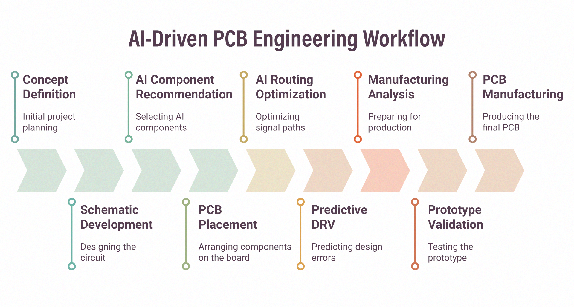
AI supports engineers throughout the design process while keeping human engineering validation at every critical stage.
How AI Reduces Design Time and Engineering Effort
Rather than simply reducing costs, AI primarily helps engineering teams shorten design cycles, minimise repetitive work, and improve overall design efficiency.
The answer depends on project complexity.
Traditional manual design generally involves:
- Higher engineering hours
- Longer development cycles
- Greater redesign costs
- Increased prototype iterations
AI-assisted design often reduces:
- Layout time
- Engineering rework
- Prototype revisions
- Time-to-market
Limitations of AI in Electronic Design
Despite rapid advancements, understanding the limitations of AI in electronic design is essential.
Engineering Judgment Cannot Be Replaced
AI identifies patterns but lacks contextual engineering reasoning.
Human engineers understand customer requirements, certification standards, reliability expectations, and product-specific trade-offs that AI cannot fully interpret.
Limited Understanding of Novel Designs
AI performs best when trained using large datasets.
Completely new technologies or unique product architectures may require entirely manual engineering decisions.
Regulatory Compliance
Industries such as aerospace, defense, healthcare, and automotive require extensive validation and documentation.
Human review remains mandatory even when AI generates design recommendations.
Data Quality Matters
Poor-quality design datasets produce unreliable AI recommendations.
Organizations must ensure their historical engineering data is accurate before adopting AI-driven workflows.
Limited Access to Proprietary Design Data
One of the biggest barriers to AI adoption in electronic design is the limited availability of proprietary engineering data. Many semiconductor manufacturers, IC vendors, and EDA software providers do not allow their design platforms or datasets to be used for AI training because of intellectual property concerns and the desire to develop their own AI-powered design solutions. As a result, many current AI tools rely primarily on publicly available or open-source hardware architectures, limiting their effectiveness for specialized or proprietary designs.
AI Adoption Is Still in Its Early Stages
AI-assisted electronic design is still evolving and has not yet become mainstream across the electronics industry. AI-powered EDA platforms often require premium licensing and specialised implementation, making adoption difficult for many small and mid-sized engineering teams. As the technology matures, costs are expected to decrease, capabilities will improve, and adoption will become more widespread. Until then, AI should be viewed as an engineering assistant rather than a replacement for traditional design expertise.
Real-World Industry Direction
Leading EDA vendors are actively integrating artificial intelligence into their platforms, enabling engineers to automate repetitive tasks while maintaining complete oversight of design decisions. Emerging concepts such as agentic EDA are pushing this evolution further by introducing AI agents capable of coordinating multiple engineering tasks, suggesting design improvements, and managing portions of the workflow under human supervision.
Across industries such as automotive electronics, industrial automation, telecommunications, and consumer devices, engineering teams increasingly rely on AI-assisted design to shorten development cycles without sacrificing product quality. This trend is particularly valuable where rapid innovation, shorter product lifecycles, and increasing design complexity demand greater efficiency.
Companies like MicroLOGIX demonstrate how experienced engineering teams combine AI-assisted design with rigorous engineering review, simulation, and validation to develop reliable electronic products.
Future of AI in Electronic Design
Although AI-assisted electronic design is gaining momentum, it has not yet become a mainstream engineering practice. Emerging technologies such as agentic EDA, AI-assisted simulation, generative PCB layouts, and digital twins are expected to further streamline electronic product development. Rather than replacing engineers, these innovations will strengthen engineering decision-making, reduce development complexity, and accelerate the delivery of reliable electronic products.
Conclusion
The future of electronics engineering is not about choosing between AI and traditional design but combining the strengths of both. While AI in electronic design accelerates design, improves accuracy, and reduces repetitive tasks, experienced engineers remain essential for innovation, validation, and compliance. Organisations that combine AI-assisted design with experienced engineering expertise will be better positioned to reduce design iterations, improve product quality, and shorten development cycles while maintaining reliability and compliance.
Frequently Asked Questions
-
What is AI in electronic design?
AI in electronic design uses machine learning and intelligent automation to support PCB layout, routing, verification, and design optimization, helping engineers work faster while maintaining engineering quality.
-
How does AI differ from traditional electronic design?
Traditional design relies mainly on manual engineering decisions, while AI assists by automating repetitive tasks, improving optimisation, and identifying design issues earlier in the workflow.
-
Can AI replace PCB design engineers?
No. AI supports engineers by improving efficiency and reducing repetitive work, but experienced professionals are still required for architecture, validation, compliance, and final design decisions.
-
What are the benefits of AI in PCB design?
AI improves component placement, intelligent PCB routing, design verification, and overall design optimisation, helping engineering teams reduce iterations and shorten development cycles.
-
What are the limitations of AI in electronic design?
AI depends on quality data and cannot replace engineering judgement, regulatory compliance reviews, or application-specific decision-making required for complex electronic products.
-
Is AI useful for embedded system design?
Yes. AI supports embedded system design by assisting with processor selection, firmware optimisation, hardware-software integration, and early identification of potential design issues.
-
Does AI reduce PCB development costs?
AI can reduce overall project costs by minimising engineering rework, shortening design cycles, reducing prototype revisions, and improving engineering productivity on complex projects.
-
Should companies adopt AI or traditional electronic design?
Most organisations achieve the best results by combining AI-assisted design with experienced engineering expertise, balancing automation, innovation, compliance, and product reliability.
-
Can AI improve Design Rule Check (DRC) accuracy?
Yes. AI predicts potential DRC violations during PCB layout instead of waiting until final verification. This helps engineers resolve issues earlier and reduces costly redesigns.
-
Which industries benefit most from AI-assisted electronic design?
Industries like automotive, aerospace, healthcare, industrial automation, telecommunications, and IoT benefit from AI by accelerating development while maintaining quality, safety, and compliance.