In electronics manufacturing, most product failures do not start in the field. They start much earlier, during PCB assembly. A misaligned component, a weak solder joint, or a hidden void under a BGA can pass unnoticed through basic checks and only fail months later in real-world conditions. This is why PCB assembly quality control is one of the most critical responsibilities for any electronics manufacturer.
As assemblies become denser and component packages shrink, traditional inspection methods struggle to keep up. Manual visual checks and random sampling simply cannot provide the consistency or coverage needed today. This is where advanced PCB inspection methods, specifically automated optical inspection (AOI) and X-ray inspection of PCB assembly, play a defining role.
Used correctly, these inspection technologies do more than catch defects. They create visibility into the manufacturing process and support long-term reliability, cost control, and trust with customers.
Table of Contents
Why PCB Assembly Quality Control Is No Longer Optional
Modern electronics are unforgiving. Fine-pitch components, multilayer boards, and leadless packages leave little room for error. Even small variations in solder paste printing or reflow profiles can lead to defects in PCB manufacturing that are difficult to detect but costly to fix later.
Quality control in electronics manufacturing must now address three key realities:
- Defects are increasingly microscopic and often hidden beneath components.
- Production volumes demand inspection at speed without sacrificing accuracy.
- Failures today are often latent, appearing only after thermal cycling, vibration, or extended use.
AOI and X-ray inspection were adopted precisely because they address these challenges in ways older inspection approaches cannot.
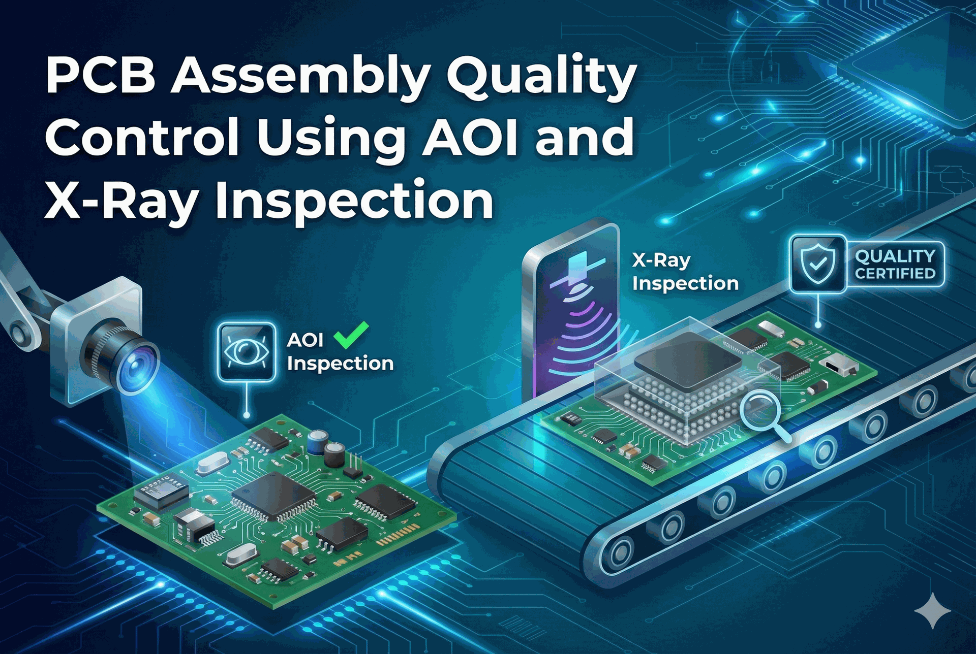
Automated Optical Inspection (AOI): The First Line of Defense
What AOI Actually Does on the Production Floor
Automated optical inspection AOI systems use high-resolution cameras and controlled lighting to examine assembled PCBs. The system compares what it sees against design data or a known-good reference to identify deviations.
In practical terms, AOI acts as a tireless inspector. It looks at every board, every time, without fatigue or subjectivity. This makes automated optical inspection PCB systems especially effective for maintaining consistency in high-volume or high-mix production.
Defects AOI Is Best At Finding
AOI excels at identifying visible and placement-related issues. These include insufficient or excessive solder, solder bridges, misaligned components, tombstoning, lifted leads, and missing or incorrect parts.
These defects directly affect electrical continuity and mechanical stability. Catching them early prevents unnecessary downstream testing failures and rework.
Where AOI Fits in the Assembly Process
AOI delivers the most value when used strategically rather than as a single checkpoint. Pre-reflow AOI focuses on solder paste quality and component placement accuracy. Post-reflow AOI examines solder joint shape, fillet formation, and overall assembly quality.
Manufacturers that use AOI feedback to fine-tune stencil design, placement accuracy, and reflow profiles often see measurable improvements in yield and process stability.
X-Ray Inspection of PCB Assembly: Seeing What AOI Cannot
Why X-Ray Inspection Is Critical for Modern Designs
As soon as assemblies include BGAs, QFNs, or other leadless packages, visual inspection reaches its limits. X-ray inspection of PCB assembly allows manufacturers to look inside solder joints and internal structures without destroying the board.
X-ray systems reveal density variations within solder joints, making it possible to identify internal defects that would otherwise remain hidden until failure.
BGA X-Ray Inspection and Hidden Defects
BGA X-ray inspection is one of the most important applications of X-ray technology. Because BGA solder balls sit entirely under the package, AOI cannot evaluate them. X-ray inspection makes it possible to detect voiding, insufficient solder volume, head-in-pillow defects, and misaligned balls.
These issues are common contributors to intermittent failures, especially in products exposed to heat cycling or mechanical stress.
Supporting Reliability and Failure Analysis
In addition to the detection of defects, the X-ray inspection of solder joints enables more in-depth analysis of reliability. Voids and collapse trends may indicate issues in reflow profile and solder paste or component handling.
This data often feeds into reliability tests for PCB validation and electronics failure analysis, helping teams address root causes instead of repeatedly fixing symptoms.
The Role of Moisture Sensitivity Level (MSL) in PCB Assembly Quality
PCB assembly quality is influenced not only by inspection capability but also by how components are handled before assembly. Moisture Sensitivity Level (MSL) is a critical consideration for BGA and QFN packages, which can absorb moisture during storage and handling. When these components are exposed to reflow temperatures, absorbed moisture expands within the package and can result in internal delamination or micro-cracking. These defects are often latent and may not be detected during initial inspection or testing.
MSL Impact on BGA and QFN Solderability
Improper MSL control also affects solder joint formation. Excess moisture exposure promotes oxidation on BGA solder balls and QFN terminations, reducing solder wetting during reflow. This increases the likelihood of non-wetting conditions, head-in-pillow defects, and mechanically weak solder joints. Such issues may not be evident through visual inspection and are frequently identified only through X-ray inspection as abnormal voiding or inconsistent solder joint formation.
AOI and X-Ray Inspection Work Best Together
AOI and X-ray inspection are not alternatives. They are complementary.
AOI delivers quick and economical inspection for visible defects on each board. X-ray inspection offers information about hidden solder joints and hidden structures, which are not observable by AOI.
Relying on only one method leaves gaps in PCB assembly quality control. A layered inspection strategy closes those gaps and reduces the risk of escaped defects reaching the customer.
Practical Use in Real Manufacturing Environments
In real production settings, inspection strategies must balance risk, cost, and throughput. For example, during a complex industrial control project, MicroLOGIX implemented inline AOI after placement and post-reflow AOI for all boards, while applying X-ray inspection selectively to BGA-heavy assemblies. This approach reduced false failures during functional testing and improved early detection of process drift.
In another case involving power electronics, X-ray inspection data revealed recurring voiding patterns that were traced back to stencil aperture design. Adjusting the stencil eliminated the issue without changing materials or equipment, improving long-term thermal reliability.
These examples show how PCB inspection equipment becomes a process improvement tool rather than just a quality gate.
Integrating Inspection Data into Quality Systems
Inspection results are most valuable when they are not isolated. Today’s AOI and X-ray systems are able to interface with manufacturing execution systems so that traceability and statistical analysis can be done.
This data enables proactive quality control in electronics manufacturing, allowing teams to spot trends before failures. It also strengthens supplier audits, design-for-manufacturing decisions, and customer confidence.
Limitations and Best Practices
AOI systems require careful programming to avoid false positives, particularly with complex or cosmetic variations. X-ray inspection requires trained operators who understand acceptable solder joint characteristics versus true defects.
The best results come from aligning inspection depth with product risk. Safety-critical or high-reliability assemblies demand tighter inspection thresholds, while lower-risk products may use selective inspection to control costs.
Regular calibration, operator training, and review of inspection criteria are essential for maintaining long-term effectiveness.
Final Takeaway
PCB assembly quality control is no longer about catching obvious mistakes. It is about building confidence that every assembly will perform reliably in real-world conditions.
Automated optical inspection (AOI) and X-ray inspection of PCB assembly offer the necessary insight to handle today’s increasingly complex PCBs and ever-reducing tolerances. By combining AOI and X-ray inspection, there is a powerful inspection infrastructure that can help eliminate errors and guarantee continuous enhancement.
For the long-term manufacturer who values performance and integrity, disciplined inspection is not an overhead. It is an investment in reliability and reputation.
FAQs
1. What is AOI in PCB assembly and how does it work?
AOI is a camera-based inspection system that checks assembled PCBs for visible placement and soldering defects by comparing board images with design data or reference standards.
2. What types of defects can AOI detect during PCB assembly?
AOI detects visible defects such as missing or incorrect components, solder bridges, insufficient or excess solder, component misalignment, tombstoning, and polarity errors.
3. What is the purpose of automated optical inspection in PCB manufacturing?
The purpose of AOI is to detect assembly defects early, ensure consistent build quality, reduce rework, and provide process feedback during PCB manufacturing.
4. How accurate is AOI compared to manual PCB inspection?
AOI is more accurate and consistent than manual inspection because it applies the same criteria to every board and does not suffer from human fatigue or subjectivity.
5. What is PCB assembly quality control and why is it important?
PCB assembly quality control ensures assembled boards meet reliability and performance requirements by identifying defects early and preventing failures during real-world operation.
6. How do manufacturers check PCB assembly quality during production?
Manufacturers use AOI, X-ray inspection, and electrical testing at different production stages to detect defects early and maintain consistent PCB assembly quality.
7. What tools are used in PCB assembly inspection and quality control?
Common tools include automated optical inspection systems, X-ray inspection systems, solder paste inspection equipment, and electrical or functional test systems.
8. What are the methods of PCB visual inspection used in electronics manufacturing?
PCB visual inspection methods include manual inspection, microscope-assisted inspection, and automated optical inspection for surface-level defect detection.
9. What is PCB inspection and how does it prevent manufacturing defects?
PCB inspection identifies assembly defects early, allowing corrective action before shipment and reducing the risk of failures, rework, and warranty issues.
10. How do manufacturers test PCBs for faults and hidden defects?
Manufacturers test PCBs using AOI for visible defects, X-ray inspection for hidden solder joints, and electrical testing to verify connectivity and functionality.